Evanescent Waveguide Couplers: Principles, Design, and Simulation Using Ansys Lumerical
How evanescent coupling transfers optical power between closely spaced waveguides, what sets the coupling length, and how Ansys Lumerical MODE is used to analyze and design these devices.
AP
Akankshya Panigrahi
Sep 4, 20267 min read
As photonic integrated circuits (PICs) continue to evolve, the ability to efficiently control and route optical power between waveguides has become increasingly important. Evanescent waveguide couplers provide a compact and effective approach for transferring optical power from one waveguide to another without requiring the waveguides to physically intersect.
These couplers are widely used in integrated photonics for applications such as power splitting, optical switching, interferometers, wavelength filtering, and coherent optical circuits. Their operation is based on the interaction between the evanescent fields of two closely spaced waveguides.
This article explains the operating principle of evanescent coupling, the parameters that determine coupling efficiency, and how Ansys Lumerical MODE can be used to analyze and design such devices.
Section 01What is an Evanescent Waveguide Coupler?
An optical waveguide confines light within a high-refractive-index region. However, the optical field does not abruptly become zero at the boundary of the waveguide. A small portion of the field extends into the surrounding material as an evanescent field.
When two waveguides are placed sufficiently close to each other, the evanescent field of one waveguide overlaps with the second waveguide. This overlap enables optical power to transfer between the two guides.
A simple implementation is a directional coupler, consisting of two parallel waveguides separated by a small gap.
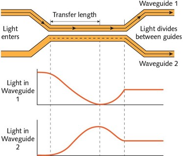
Transfer length and power exchange between the two guides
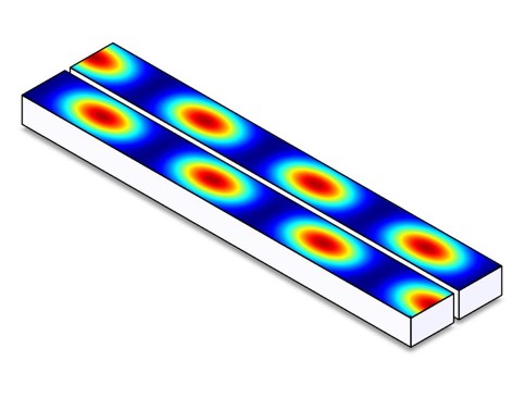
Optical power alternating between the coupled waveguides
If light is initially launched into Waveguide 1, the optical power gradually transfers to Waveguide 2 as the light propagates through the coupling region. With an appropriate combination of waveguide separation and coupling length, designers can achieve a desired power split, such as 50:50 or nearly 100% transfer.
The coupling process is periodic, meaning that the power can transfer back and forth between the two waveguides.
Section 02How Does Evanescent Coupling Work?
The simplest way to understand the coupling mechanism is through the modes of the combined waveguide structure.
When two identical waveguides are sufficiently close, the system supports two coupled modes, commonly referred to as the even and odd supermodes. These modes have slightly different effective refractive indices.
The difference between their effective indices can be written as:
Δn = n₁ − n₂
where n₁ and n₂ are the effective indices of the two coupled modes.
Because these modes propagate with different phase velocities, their relative phase changes along the propagation direction. This changing phase produces the periodic transfer of optical power between the waveguides.
For an ideal symmetric coupler, the power transferred to the second waveguide can be expressed as:
P₂(L) = P₀ sin²(πLΔn / λ₀)
where:
P₀ is the input optical power
P₂(L) is the power in the second waveguide after propagation distance L
Δn is the effective-index difference between the coupled modes
λ₀ is the free-space wavelength
L is the coupling-region length
This relationship shows an important design principle: the coupling length is directly determined by the effective-index difference between the coupled modes.
For complete power transfer, the required length is:
L100% = λ₀ / 2Δn
For example, in the Ansys Lumerical example, the effective-index difference is approximately 0.06016 at a wavelength of 1.55 μm. This gives a calculated 100% coupling length of approximately 12.88 μm.
Section 03Why Waveguide Gap Matters
One of the most important parameters in an evanescent coupler is the gap between the waveguides.
As the waveguides are brought closer together, their evanescent fields overlap more strongly. This generally increases the coupling strength and reduces the length required to transfer a given amount of optical power.
Conversely, increasing the gap reduces the field overlap and therefore increases the coupling length.
This creates an important practical challenge. Although a smaller gap can provide stronger coupling and a more compact device, it can also make the coupler more sensitive to fabrication variations.
Small deviations in waveguide separation caused by lithography or etching can change the coupling coefficient and consequently alter the final power-splitting ratio. Therefore, the nominal design should not be considered in isolation; fabrication tolerance should also be considered during the design process.
Section 04Simulating an Evanescent Coupler in Ansys Lumerical MODE
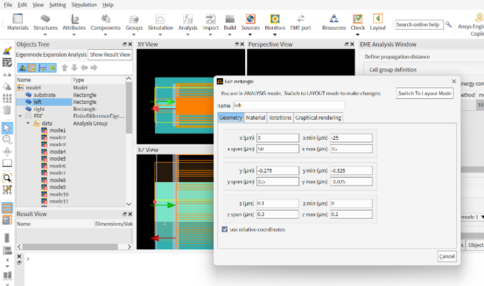
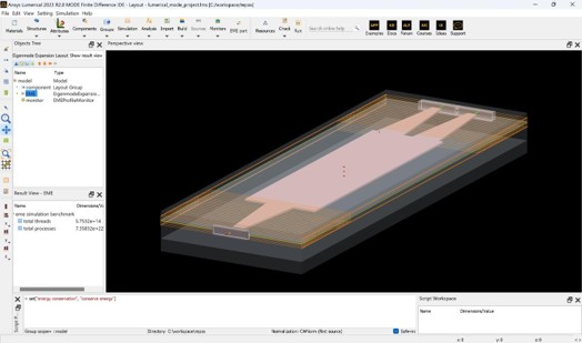
Ansys Lumerical MODE provides several approaches for analyzing evanescent waveguide couplers. The example provided by Ansys uses two silicon-on-insulator (SOI) waveguides, each 500 nm wide and 200 nm thick, with a 50 nm separation between them. Because the coupling is highly sensitive to the gap, a fine mesh is used in the region between the waveguides.
A typical simulation workflow can be summarized as follows:
1. Define the waveguide geometry
The first step is to create the two waveguides and define the relevant material properties. For an SOI platform, silicon can be used as the waveguide material with silicon dioxide as the surrounding material.
2. Calculate the coupled modes
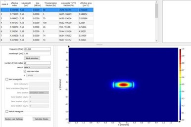
The Finite Difference Eigenmode (FDE) solver can be used to calculate the modes supported by the coupled waveguide structure.
Instead of considering each waveguide independently, the FDE solver analyzes the complete cross-section containing both waveguides. The resulting even and odd modes provide the effective indices required to calculate the coupling length.
3. Calculate the coupling length
Once n₁ and n₂ are obtained, their difference can be used in the analytical coupling equation.
This provides a quick estimate of the required coupling-region length before performing a full propagation simulation.
4. Verify the result using propagation
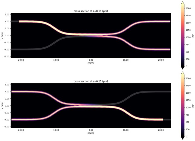
The calculated coupling length can then be verified using a propagation-based simulation. The optical field can be monitored as it travels through the coupling region, allowing the periodic transfer of power between the two waveguides to be visualized.
Section 05Choosing Between FDE, EME, and varFDTD
One of the useful aspects of the Lumerical example is that the same coupler can be investigated using multiple simulation approaches.
FDE is particularly useful for calculating the modes and effective indices of the coupled structure. Since it calculates the full 2D mode profiles, it can provide accurate modal information for a uniform cross-section.
EME (Eigenmode Expansion) can be used to model propagation through the device by expanding the optical field into eigenmodes. It is especially useful when analyzing longer structures or devices containing different sections. In the referenced example, EME predicts a coupling length of approximately 12.7 μm, in good agreement with the analytical result.
varFDTD provides another propagation-based approach. However, its treatment of the waveguide cross-section involves approximations, and the effective-index difference may differ from that obtained using a full 2D eigenmode calculation. Consequently, the resulting coupling length can require careful interpretation or calibration.
For the specific example documented by Ansys, the reported coupling lengths are approximately:
Method
Coupling Length
FDE + analytical calculation
12.88 μm
FDE + propagation
~13 μm
EME
~12.7 μm
varFDTD
~12.5 μm*
*The varFDTD result involves adjustment of the waveguide gap to obtain a comparable effective-index difference.
This comparison demonstrates that different simulation approaches can provide closely matching results when the appropriate assumptions and settings are used.
Section 06What About Non-Uniform Coupling Regions?
Real photonic devices do not always consist of two perfectly parallel waveguides with a constant cross-section. Tapers, bends, transitions, and other geometrical variations may be introduced to improve performance or reduce the footprint.
For small variations, FDE can still provide useful modal information and an approximate understanding of the coupling behavior. However, a simple propagation calculation based on a uniform cross-section does not fully capture these variations.
For devices with significant non-uniformity, simulation methods such as EME, varFDTD, or full 3D FDTD can be used to model the complete structure more accurately.
Section 07Applications of Evanescent Waveguide Couplers
Evanescent couplers form an important building block for many photonic integrated circuits. By controlling the coupling coefficient and coupling length, designers can create:
50:50 optical power splitters
Directional couplers
Mach–Zehnder interferometers
Optical switches
Ring resonator coupling sections
Wavelength-selective devices
Integrated sensors
Coherent optical circuits
Photonic signal-processing components
Their compact footprint and compatibility with planar fabrication make them particularly attractive for silicon photonics and other integrated photonic platforms.
Conclusion
Evanescent waveguide couplers provide a powerful mechanism for controlling optical power on a photonic chip. Their operation relies on the overlap of the evanescent fields of closely spaced waveguides and the interference between the resulting coupled modes.
The waveguide gap, coupling length, wavelength, modal effective indices, and fabrication tolerances are key factors that determine the final device performance.
Ansys Lumerical MODE offers a practical workflow for studying these devices, starting with FDE-based modal analysis and analytical coupling-length calculations and extending to EME, varFDTD, or FDTD simulations for more complex structures. The ability to compare analytical predictions with numerical simulations makes Lumerical particularly useful for understanding the physics as well as optimizing practical photonic designs.
Found this useful? Share it
Continue Reading
More from our engineers.
If this article was useful, these picks up where it leaves off — practical reads from the CADFEM engineering practice.