Understanding Terrain-Based Mission Analysis and Terrain Fidelity with Ansys STK
When engineers think about mission analysis, attention naturally goes to the vehicle, trajectory, sensor, communications system, or target.
Read Article →
Wide-bandgap semiconductors such as GaN and SiC are reshaping electric vehicles, renewable energy, aerospace and consumer electronics — and Ansys simulation is catalyzing their real-world impact.

Imagine an electric vehicle that recharges in under 15 minutes, mirroring the convenience of conventional fueling or a palm-sized laptop adapter that remains cool even during intense workloads. These are no longer far-fetched dreams, but rapidly advancing realities, enabled by the disruptive capabilities of Gallium Nitride (GaN) and Silicon Carbide (SiC) semiconductors.
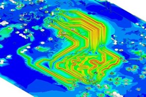

For decades, silicon has been the industry standard in power electronics. But as global demand escalates for compact, efficient, and high-speed systems, silicon is reaching the upper bounds of its performance envelope. In this context, wide-bandgap semiconductors such as GaN and SiC are emerging as pivotal technologies reshaping paradigms across electric vehicles, renewable energy infrastructure, aerospace, and high-performance consumer electronics.
What precisely makes these materials the cornerstone of next-generation power solutions? Let's delve into their scientific foundations, industrial applications, and how simulation platforms like Ansys are catalyzing their real-world impact.

The story of GaN and SiC is interwoven with the broader evolution of power electronics — a field driven by the imperative to achieve higher voltage thresholds, enhanced thermal stability, and faster switching frequencies. While silicon laid the groundwork, its material constraints sparked the pursuit of alternatives.
Key Developmental Milestones:
These milestones didn't just improve existing technologies — they enabled innovations once considered unfeasible.
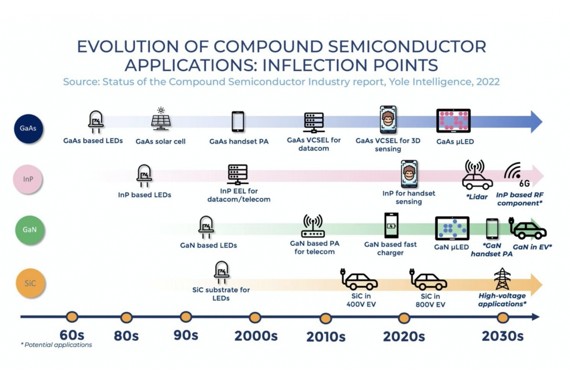
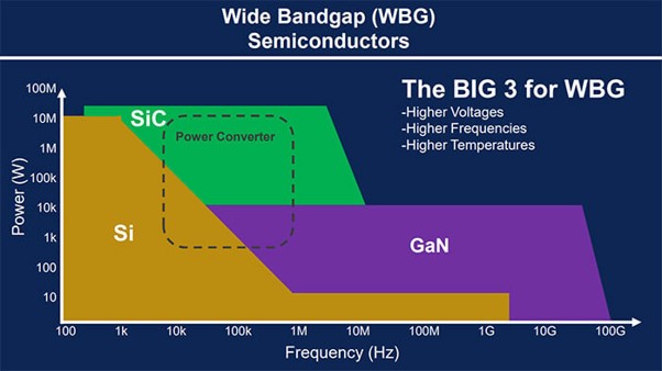
At the core of GaN and SiC's game-changing performance lies their wide bandgap structure. Unlike silicon, which has a bandgap of 1.1 eV, GaN (3.4 eV) and SiC (3.3 eV) can tolerate much higher electric fields, operate at elevated temperatures, and conduct electricity with far greater efficiency.
| Property | Silicon (Si) | Silicon Carbide (SiC) | Gallium Nitride (GaN) |
|---|---|---|---|
| Bandgap (eV) | 1.1 | 3.3 | 3.4 |
| Thermal Conductivity (W/mK) | 150 | 370 | 130 |
| Critical Electric Field (MV/cm) | 0.3 | 3.0 | 3.5 |
| Max Junction Temperature (°C) | 150 | 600 | 400 |
| Electron Mobility (cm²/Vs) | 1400 | 900 | 2000 |
The superior thermal and electrical properties of these semiconductors make them indispensable for high-power, high-frequency, and thermally constrained environments.
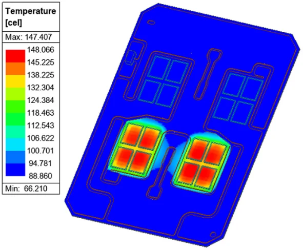
While GaN and SiC offer remarkable intrinsic advantages, realizing their full potential requires meticulous system-level optimization. This is where Ansys simulation platforms become indispensable, enabling engineers to model, simulate, and validate every nuance of thermal, electromagnetic, and power behavior before prototyping.
Key Ansys Tools in Action:
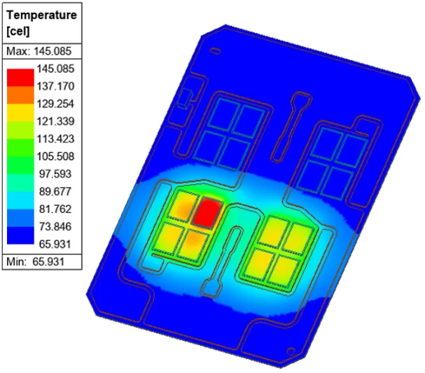
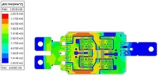
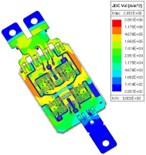
GaN and SiC semiconductors are not just the future, they are the present of power electronics innovation. As the world pivots to smarter, faster, and more energy-conscious solutions, these materials will underpin everything from zero-emission transportation to orbital communications.
Ansys simulation ecosystems enable this transformation by bridging the gap between material potential and practical design, allowing engineers to validate, optimize, and scale disruptive technologies with confidence.
 DME
When engineers think about mission analysis, attention naturally goes to the vehicle, trajectory, sensor, communications system, or target.
Read Article →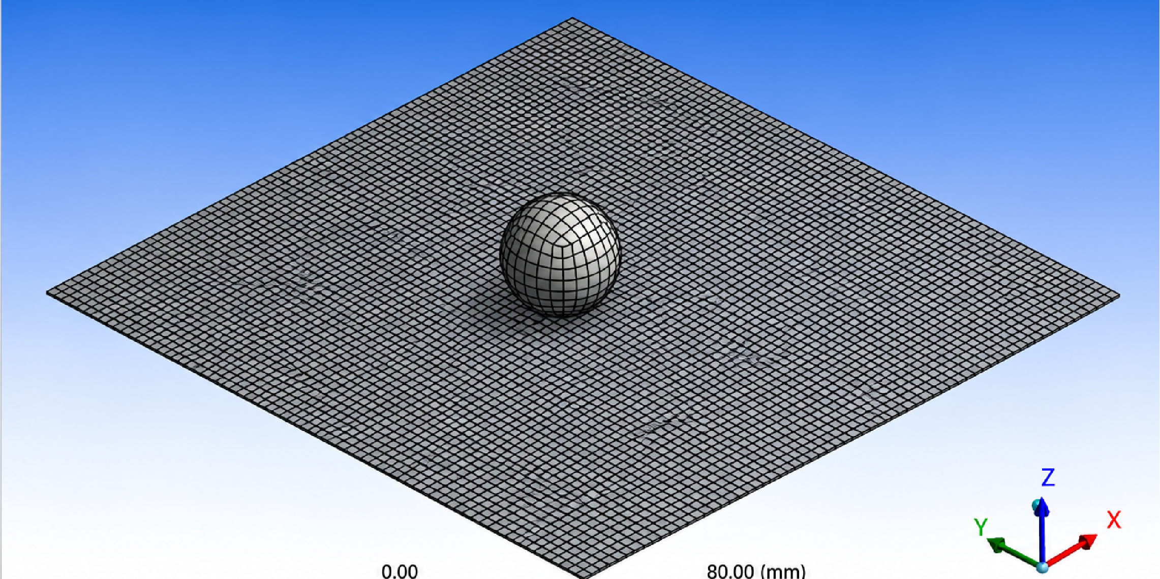 Structures
Laminated composite materials such as fiber reinforced polymers (FRPs) offer exceptional strength-to-weight ratios, making them essential in aerospace, defense, and automotive engineering.
Read Article →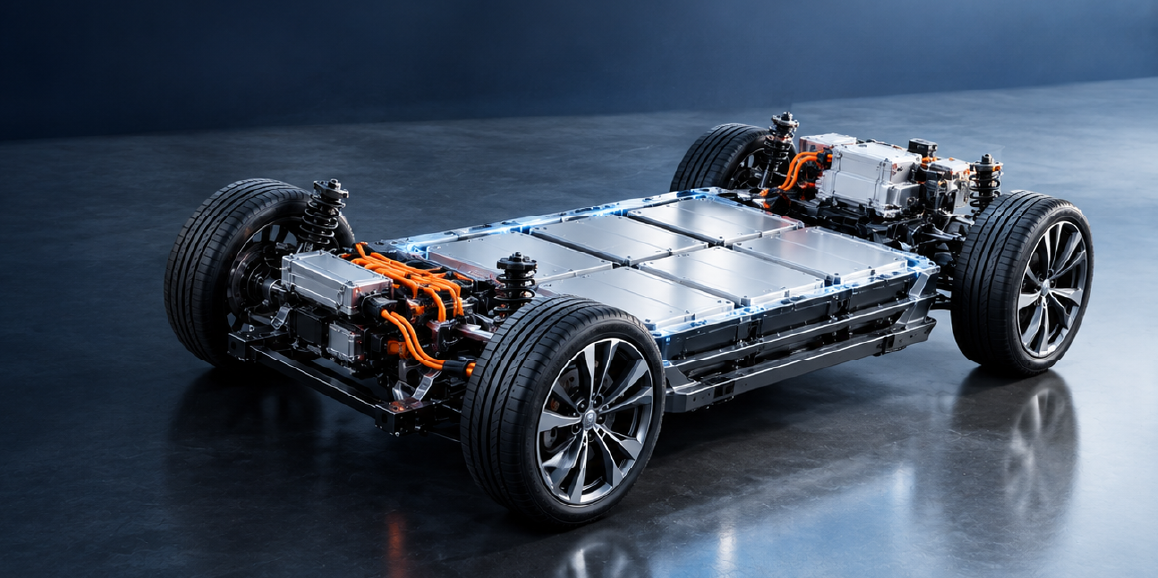 Multi Physics
Read the CADFEM guide to smart BMS functions, automotive thermal management, centralized vs. modular architectures, and Ansys simulation
Read Article →Connect with CADFEM experts for advanced simulation, automation, and engineering solutions tailored to your industry.